[5]沈桂英, 赵有文, HE Jianjun. Structural Characterization of Carbon-implanted GaSb[J]. Journal of Wuhan University of Technology(Materials Science), 2023, 38 (5): 969-973.
[8]Zhao, Youwen.Evaluation of residual stress in InP and InAs (100) substrates obtained from single crystals grown by LEC and VGF methods), Mater. Sci. Semicond. Pro., 2021, 通讯作者
[9]Zhao, Youwen.Residual stress distribution and flatness of dislocation-free Te-GaSb (100) substrate, Jpn. J. Appl. Phys., 2021, 通讯作者
[10]Zhao, Youwen.Evaluation of LEC and VGF-InAs substrates through surface defect characyerization and epitaxy growth), Mater. Sci. Semicond. Pro., 2021, 第 2 作者
[16]余丁,沈桂英,谢辉,刘京明,孙静,赵有文.Mechanism of free electron concentration saturation phenomenon in Te-GaSb single crystal[J].Chinese Physics B,2019,28(05):267-271, 通讯作者
[18]Zhao, Youwen Wet etching generation of dislocation pits with clear facets in LEC-InAs, Journal of Crystal Growth, 2019, 通讯作者
[19]Zhao, Youwen.Photoluminescene study acceptor defects in lightly doped n type, Journal of Semiconductors, 2019, 第 2 作者
[20] Zhao, Youwen.impurity band conduction in Mn-doped p type InAs single crystal, Materials Science in Semiconductor Processing, 2018, 第 2 作者
[21]Zhao, Youwen. LVM Spectroscopy Investigation of Complex Defects in InAs single crystals grown by the LEC Method, Journal of Electronic materials, 2018, 第 2 作者
[22]Zhao, Youwen 退火Te-GaSb的电学性质, Electrical and optical property of annealed Te-doped GaSb, Journal of Semiconductors, 2017, 通讯作者
[23]赵有文,段满龙,卢伟,杨俊,董志远,刘刚,高永亮,杨凤云,王风华,王俊,刘京明,谢辉,王应利,卢超. 4 inch低位错密度InP单晶的VGF生长及性质研究[J]. VGF growth of 4 inch diameter InP with low dislocation density and property investigation, 人工晶体学报, ,2017,46(05):792-796.
[24]杨俊,段满龙,卢伟,刘刚,高永亮,董志远,王俊,杨凤云,王凤华,刘京明,谢辉,王应利,卢超,赵有文.4英寸低位错密度GaSb单晶生长及高质量衬底制备, growth of 4 inch diameter GaSb single crystal with low dislocation density and high quality substrate preparation, 人工晶体学报,2017,46(05):820-824. 通讯作者
[25] 通过消除原生缺陷提高InAs单晶的透光率, Enhancement of below gap transmission of InAs single crystal via suppression of native defects, Mater. Res. Express, 2017, 通讯作者
[26]Bai Yong-Biao; Zhao You-Wen*; Shen Gui-Ying; Chen Xiao-Yu; Liu Jing-Ming; Xie Hui; Dong Zhi-Yuan; Yang Jun; Yang Feng-Yun; Wang Feng-Hua.N-type GaSb single crystals with high below-band gap transmission[J].Chinese Physics B,2017,26(10):446-449.通讯作者
[28]苏杰,刘彤,刘京明,杨俊,沈桂英,白永彪,董志远,赵有文.Carbon agent chemical vapor transport growth of Ga2O3 crystal[J].Journal of Semiconductors,2016,37(10):47-51.通讯作者
[29]Performance improvement of c-Si solar cell by a combination of SiNx/SiOx passivation and double P-diffusion gettering treatment, Journal of Semiconductors, 2017, 通讯作者
[30]晶硅电池的黑斑缺陷, black spot defect in c-Si solar cell, 半导体光电, 2016, 通讯作者
[31]苏杰,刘彤,刘京明,杨俊,白永彪,沈桂英,董志远,王芳芳,赵有文.Thermally induced native defect transform in annealed GaSb[J].Chinese Physics B,2016,25(07):454-458.
[32]曹可慰,刘彤,刘京明,谢辉,陶东言,赵有文,董志远,惠峰.Evaluation of four inch diameter VGF-Ge substrates used for manufacturing multi-junction solar cell[J].Journal of Semiconductors,2016,37(06):25-30.
[34]曹可慰,刘彤,刘京明,谢辉,陶东言,赵有文,董志远,惠峰. Evaluation of four inch diameter VGF-Ge substrates used for manufacturing multi-junction solar cell[J]. 半导体学报:英文版,2016,0(6).
[35]苏杰,刘彤,刘京明,杨俊,沈桂英,白永彪,董志远,赵有文. Carbon agent chemical vapor transport growth of Ga2O3 crystal[J]. .Journal of Semiconductors,2016,37(10):47-51.
[36]Xie Hui; Zhao Youwen*; Liu Tong; Dong Zhiyuan; Yang Jun; Liu Jingming..C-H complex defects and their influence in ZnO single crystal[J].Chinese Physics B,2015,24(10):511-513., 通讯作者
[37]Tao Dongyan*; Cheng Yu; Liu Jingming; Su Jie; Liu Tong; Yang Fengyun; Wang Fenghua; Cao Kewei; Dong Zhiyuan; Zhao Youwen.Chemical and electrical properties of(NH4)2S passivated GaSb surface[J].Journal of Semiconductors,2015,36(07):49-53.
[38]Xie Hui*; Liu Tong; Liu Jingming; Cao Kewei; Dong Zhiyuan; Yang Jun; Zhao Youwen。Implantation induced defects and electrical properties of Sb-implanted ZnO.SCIENCE CHINA-TECHNOLOGICAL SCIENCES, 2015, 58(8): 1333-1118.
[39]Dongyan Tao; Yu Cheng; Jingming Liu; Jie Su; Tong Liu; Fengyun Yang; Fenghua Wang; Kewei Cao; Zhiyuan Dong; Youwen Zhao*.Improved surface and electrical properties of passivated GaSb with less alkaline sulfi de solution. Materials Sciencein Semiconductor Processing, 2015, 40: 685-689.
[41]Zhao, Youwen.Improved surface and electrical properties of passivated GaSb with lessalkaline sulfi de solution,, Materials Science in Semiconductor Processing, 2015, 通讯作者
[42]IZhao, Youwen.mplantation induced defects and electrical properties of Sb-implanted ZnO, SCIENCE CHINA Technological Sciences, 2015, 第 4 作者
[43]Zhao, Youwen.Evaluation of four inch diameter VGF-Ge substrate used for manufacturing Multi-junction Solar Cell, Journal of Semiconductor, 2015, 通讯作者
[46] Chen, Teng*; Zhao, Youwen; Dong, Zhiyuan; Yang, Jun; Liu, Tong. Synthesis of chalcopyrite CuIn1-xGaxSe2 alloys for photovoltaic application by a novel melting method.Materials Letters, 2013, 106: 52-55.
[47]Liu, Jingming*; Zhao, Youwen; Dong, Zhiyuan; Yang, Fengyun; Wang, Fenghua; Cao, Kewei; Liu, Tong; Xie, Hui; Chen, Teng. Improvement of the surface quality of semi-insulating InP substrates through a novel etching and cleaning method.Journal of Vacuum Science and Technology A, 2013, 31(3): 031404.
[48]Chen, Teng*; Zhao, Youwen; Dong, Zhiyuan; Liu, Tong; Wang, Jun; Xie, Hui. Analysis of solar cells fabricated from UMG-Si purified by a novel metallurgical method.Semiconductor Science and Technology, 2013, 28(1): 015024.
[49]Liu, Tong*; Dong, Zhiyuan; Zhao, Youwen; Wang, Jun; Chen, Teng; Xie, Hui; Li, Jian; Ni, Haijiang; Huo, Dianxin.Purification of metallurgical silicon through directional solidification in a large cold crucible.Journal of Crystal Growth, 2012, 355(1): 145-150.
[50]Liu, Tong*; Dong, Zhiyuan; Zhao, Youwen; Wang, Jun; Chen, Teng; Xie, Hui; Li, Jian; Ni, Haijiang; Huo, Dianxin.Large scale purification of metallurgical silicon for solar cell by using electron beam melting.Journal of Crystal Growth, 2012, 351(1): 19-22.
[51]Li Hui*; Zhou Kai; Pang Jingbiao; Shao Yundong; Wang Zhu; Zhao Youwen. Defect properties of as-grown and electron-irradiated Te-doped GaSb studied by positron annihilation , Semiconductor Science and Technology, 2011, 26(7): 075016. , 通讯作者
[69]Zhao, Y. W.*; Dong, Z. Y.. Annihilation of deep level defects in InP through high temperature annealing.Journal of Physics and Chemistry of Solids, 2008, 69(2-3): 551-554.
[70]Wei, Xuecheng; Zhao, Youwen; Dong, Zhiyuan; Li, Jinmin.Investigation of native defects and property of bulk ZnO single crystal grown by a closed chemical vapor transport method. Journal of Crystal Growth, 2008, 310(3): 639-645.
[76]Wei, Xuecheng; Zhao, Youwen; Dong, Zhiyuan; Li, Jinmin.Characterization of bulk ZnO single crystal grown by a CVT method - art. no. 68410F. Conference on Solid State Lighting and Solar Energy Technologies, China, 2007-11-12 to 2007-11-14.
[77]Zhao You-Wen*; Miao Shan-Shan; Dong Zhi-Yuan; Lue Xiao-Hong; Deng Ai-Hong; Yang Jun; Wang Bo. Thermally induced Fe atom transition from substitutional to interstitial sites in InP and its influence on material property. Acta Physica Sinica, 2007, 56(9): 5536-5541.
[78]Wang Bo; Zhao You-Wen*; Dong Zhi-Yuan; Deng Ai-Hong; Miao Shan-Shan; Yang Jun. Electron irradiation induced defects in high temperature annealed InP single crystal. Acta Physica Sinica, 2007, 56(3): 1603-1607.
[79]Zhao You-Wen*; Dong Zhi-Yuan.Generation and suppression of deep level defects in InP.Acta Physica Sinica, 2007, 56(3): 1476-1479.
[80]Shao, Y. D.; Wang, Z.*; Dai, Y. Q.; Zhao, Y. W.; Tang, F. Y..Identification of vacancies in electron irradiated GaSb by coincidence Doppler broadening spectroscopy.Materials Letters, 2007, 61(4-5): 1187-1189.
[81]Yang Jun; Zhao You-Wen*; Dong Zhi-Yuan; Deng Ai-Hong; Miao Shan-Shan; Wang Bo.Influence of deep level defects on electrical compensation in semi-insulating InP materials.Acta Physica Sinica, 2007, 56(2): 1167-1171.
[89]Y.W. Zhao, Z.Y. Dong, A.H. Deng , Electron irradiation-induced defects in InP pre-annealed at high temperature, Materials Science in Semiconductor Processing , 2006, 9(1-3): 380-383.
[90]Zhao, Youwen*; Dong, Zhiyuan; Miao, Shanshan; Deng, Aihong; Yang, Jun; Wang, Bo.Origin of deep level defect related photoluminescence in annealed InP.Journal of Applied Physics, 2006, 100(12): 123519.
[91]Zhao, YW*; Dong, ZY; Duan, ML; Sun, WR; Yang, ZX.Growth of high quality semi-insulating InP single crystal by suppression of compensation defects. Journal of Rare Earths, 2006, 24: 75-77.
[104]Zhao, YW*; Dong, HW; Li, JM; Ling, LY.Photoluminescence characteristics of InP annealed in phosphorus and iron phosphide ambiences.Materials Science in Semiconductor Processing, 2005, 8(4): 531-535.
[105]Zhao, Y. W.*; Dong, Z. Y.; Li, Ch. J. Approach for defect suppression and preparation of high quality semi-insulating InP.Journal of Crystal Growth, 2005, 275(1-2).
[109]Zhou, XL*; Zhao, YW; Sun, NF; Yang, GY; Xu, YQ; Sun, TN. Study on the perfection of in situ P-injection synthesis LEC-InP single crystals.Journal of Crystal Growth, 2004, 264(1-3): 17-20.
[113]Dong, ZY*; Zhao, YW; Zeng, YP; Duan, ML; Sun, WR; Jiao, JH; Lin, LY.Microdefects and electrical uniformity of InP annealed in phosphorus and iron phosphide ambiances.Journal of Crystal Growth, 2003, 259(1-2): 1-7.
[114]Dong, HW*; Zhao, YW; Li, JM. Annealing and activation of silicon implanted in semi-insulating InP substrates.Materials Science in Semiconductor Processing, 2003, 6(4): 215-218.
[115]Dong, HW*; Zhao, YW; Zeng, YP; Jiao, JH; Li, JM; Lin, LY. Influence of semi-insulating InP substrates on InAlAs epilayers grown by molecular beam epitaxy. Journal of Crystal Growth, 2003, 250(3-4): 364-369.
[117]Deng, AH*; Mascher, P; Zhao, YW; Lin, LY. Effects of annealing ambient on the formation of compensation defects in InP.Journal of Applied Physics, 2003, 93(2): 930-932.
[119]Y. W. Zhao, H. W. Dong, Y. H. Chen, Y. H. Zhang, J. H.Jiao, J. Q. Zhao and L. Y. Lin, S. Fung, Creation and Suppression of Point Defects through a Kick-out Substitution Process of Fe in InP, Applied Phys. Lett. s, 2002, 80(16): 2878-2879.
[120]Youwen Zhao, Niefeng Sun, Hongwei Dong, Jinghua Jiao, Jianqun Zhao, Tongnian Sun and Lanying Lin,Characterization of Defects and Whole Wafer Uniformity of Annealed Undoped Semi-insulating InP Wafers, Materials Science and Engineering B-Solid State Materials for Advanced Technology, 2002, 91: 521-524.
[121]Dong, HW*; Zhao, YW; Zhang, YH; Jiao, JH; Zhao, JQ; Lin, LY.Deep levels in semi-insulating InP obtained by annealing under iron phosphide ambiance.Journal of Applied Physics, 2002, 92(4): 1968-1970.
[122]Dong, HW*; Zhao, YW; Lu, HP; Jiao, JH; Zhao, JQ; Lin, LY. Photoluminescence assessment of undoped semi-insulating InP wafers obtained by annealing in iron phosphide vapour.Semiconductor Science and Technology, 2002, 17(6): 570-574.
[123]Ling, CC*; Mui, WK; Lam, CH; Beling, CD; Fung, S; Lui, MK; Cheah, KW; Li, KF; Zhao, YW; Gong, M. Gallium vacancy and the residual acceptor in undoped GaSb studied by positron lifetime spectroscopy and photoluminescence.Applied Physics Letters, 2002, 80(21): 3934-3936.
[124]Zhao, YW*; Dong, HW; Jiao, JH; Zhao, JQ; Lin, LY. Fe-diffusion-induced defects in InP annealed in iron phosphide ambient. Japanese Journal of Applied Physics, 2002, 41(4A): 1929-1931.
[125]Shan, YY*; Deng, AH; Ling, CC; Fung, S; Ling, CD; Zhao, YW; Sun, TN; Sun, NF.Positron-annihilation study of compensation defects in InP.Journal of Applied Physics, 2002, 91(4): 1998-2001.
[139]Y. W. Zhao, S. Fung, Y. L. Luo, and C. D. Beling, Electrical conduction of annealed semi-insulating InP, J. Appl. Phys. 87, 3838(2000)
[140]Y. W. Zhao, S. Fung, C. D. Beling, N. F. Sun, T. N. Sun, X. D. Chen, and G. Y. Yang, Effects of annealing on the electrical properties of Fe-doped InP, J. Appl. Phys. 86, 981(1999)



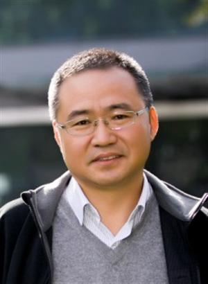 赵有文,男,博士,现任中国科学院半导体研究所研究员,博士生导师。
 教学情况:

 科学研究:
 论文专著:
 科学中国人报道: